EXAMPLE:
LAYOUT OF AN INVERTING AMPLIFIER
This example will help you to create a layout
for the inverter you designed in the first example. It will go over how to
create mosfets, resistors, and capacitors in our process.
There are many considerations to take into account when deciding how to do a
layout. This is NOT an example on layout techniques, but more of a generalized
example to help get you familiar with Virtuoso and laying-out some basic
components.
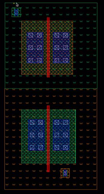
The following picture shows a layout for the inverting amplifier, ready for
extracting. The next section explains how to make each of the separate
components in Virtuoso.
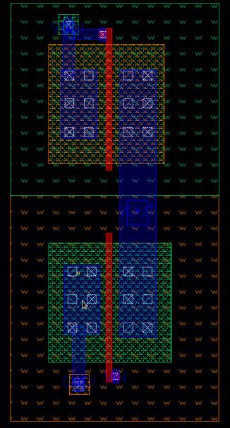
Figure 1: Layout example.
1.
Create a new cell, where you will layout the inverter:
In Library Manager:
Highlight your inverter schematic library (TEST if
that is what you chose).
File->New->Cellview
Choose library TEST, cell name "inverter", view name
"layout", and Type: Layout and Application open with " Layout L". Click
OK.
2. Laying-out
the components for your circuit:
For this inverter we will need to layout an nmos transistor and pmos transistor. The following sections will describe how to make these components.
Before beginning your layout, you will need to configure the display and editor settings. From Options -> Display you can find the display options. X and Y axis spacing is specified. Make sure all the files of the same project shares the same X Snap and Y Snap spacing to avoid grid errors. The minimum X snap and Y snap spacing in 5nm, which is 0.005um. Be sure your X Snap Spacing and Y Snap Spacing read ‘0.005’.
It will also be of interest to read the design rules for the process. We are using FreePDK45. These are the rules for spacing, minimum dimensions, etc that our layout must meet.
2.1
Layout of MOSFETs:
The design used an NMOS transistor with 60nm length and 1.2um width. The NMOS transistor uses layers pwell, active, nimplant, poly, metal1 and contact. You can start designing the transistor by selecting "active" on the LSW and drawing a rectangle on the layout editor. Note also the letters "drw", "net", and "pin" next to each entry in the LSW. These are the purposes of a shape. The purpose is used to indicate special functionality of a shape. We will be using "drw" for now.
At this point, do not worry about drawing the rectangle to exact dimensions and just draw a rectangle of any arbitrary dimension. You can zoom in and out of the editor by using the zoom Rbuttons located on the top menubar of the editor. You can also draw a box around the area you want to zoom in by holding on to your right mouse click button. When you release the button, the area you selected will be zoomed in.
Once you draw the rectangle, you can select it and press "q" or Edit->Basic->Properties to change the dimensions of the rectangle. You can also adjust the dimension by pressing "s" or Edit->Stretch You can move objects around by pressing "m" or Edit->move. Readers are strongly encouraged to get familiar with other keyboard shortcuts as this will reduce design time later on. To measure the distance between twoo points, you can press "k" or Tool->Creat Ruler. The default units are "user units" and are in microns.
Our transistor has a width of 1.2um, so make sure the width of the active layer is 1.2um. You can change the width and height by editing the properties (‘q’) or stretching (‘s’). You can check the dimensions of the transistor using a ruler (‘k’). Draw another rectangle of the nimplant layer. The active and nimplant layers must overlap, and these form the source and drain diffusion regions of the NMOS transistor we are creating.
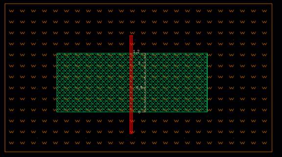
The next step is to draw the gate of the transistor. This is done by selecting "poly" in the LSW and drawing another rectangle to form the gate. Make sure that the length of the gate is set to 60nm to create the transistor that we used for the schematic. Now, we have formed the channel and the source and drain diffusion regions. The next step is to draw a pwell outside the NMOS transistor. Use the same procedure as described earlier to draw the pwell (Note that the minimum well enclosure of active is 0.055um as required by the DRC rules). The resulting transistor is shown in in the following picture.
A Note on using Fingers:
In analog design, long transistors are often split into smaller ones using ‘fingers’. This is done to both save space and decrease the gate resistance. This ‘folds’ the mos onto itself with alternating drain and source areas and multiple poly areas as the gate is split up. One finger is ok for this example, but looking in to layout with multiple fingers may be helpful for future designs.
We still have to create contacts for the source, drain and the body terminals of the transistor. This can be done by clicking on Create->Via or pressing "o" and then selecting "M1N" (for NMOS) or "M1P" (for PMOS). You can also create contacts to the active layer by selecting "contact" from the LSW and painting a rectangle on the Active layer. Paint two contacts for the Source and Drain regions of the transistor (Note that the minimum spacing between poly and M1 is 0.035um as required by the DRC rules). Now you need to create a body terminal. To do this, click on Create- >via or press "o". In the window that opens up, make sure that the Technology Library is set to NCSU_TechLib_FreePDK45 and select "PTAP" in the Via Definition field. Place the PTAP 20 connection in contact with the pwell you have drawn. You can press Shift+F to reveal the details inside the PTAP connection.
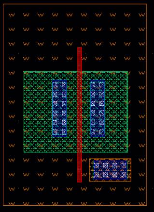
When you create an instance, you can specify the number of rows and columns, as well as the "Delta Y" and "Delta X", to create an array of the same instances. Array is highly preferred if you have a regular pattern repeating many times, e.g., an inverter chain, a long NTAP containing lots of body contacts, etc. The instance array can make your layout well organized and much cleaner. Draw metal1 rectangles over the contacts so that you can connect the terminals to other signals in your circuit. Your NMOS transistor is now ready. The final transistor should look like the following picture.
You can create the PMOS transistor similarly. It uses the following layers: nwell, active, pimplant, poly, metal1 & contact. Draw the PMOS transistor with the dimensions from the schematic. Place a PTAP in the Pwell of the NMOS transistor and an NTAP in the Nwell of the PMOS transistor. Place the PTAP by pressing Create->via and selecting NTAP or PTAP under Via Definition. You can see the details of the via by pressing Shift+f or hide the details with Ctrl+f.
The layout should somewhat resemble the following picture:
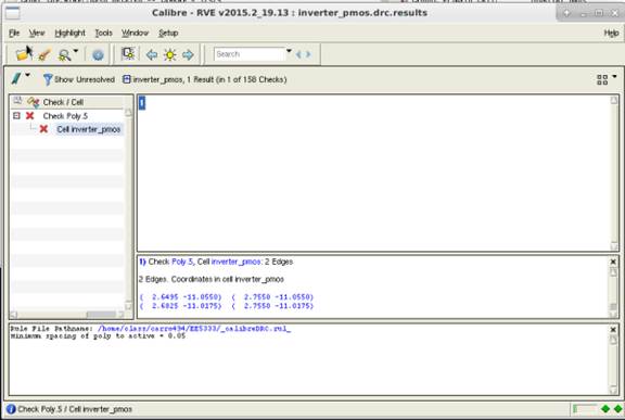
We now have the two transistor with single gate, drain, source, and bulk connections. Make sure to do DRC before continuing on to make sure everything was placed correctly. Run a DRC by Calibre-> Run DRC…. Select run DRC. After the DRC runs, you can select the filter button to ‘Show Unresolved’ so that you can see DRC violations. Fix your DRC violations. You can click on each violation for a description.
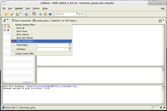
Filtering for Unresolved DRC Errors
Details
of Unresolved Error
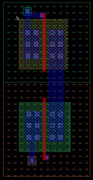
Make the appropriate connections that reflect the schematic. Connect the sources using metal. To make a connection to a Poly layer, place a via and select the M1-Poly for your via definition. Your NTAP will be connected to VDD, and your PTAP will be connected to ground. Your layout should resemble the picture below:
3.
Routing and Adding Pins:
Now that we have all the components we need to make our inverter, we can simply move them around and route the correct connections. As mentioned earlier, this example is less focused on the techniques used for layout, and more on how to make some general components and get the reader familiar with using the tool. However, a couple quick pointers will be given here.
- When putting together your layout, place large metal rectangles (metal2 works well) along the top and botttom for your Vdd and Gnd rails. Try to place all of your layout within these rails. Also, when connecting to these (or any routing connection really) its always a good idea to put as many via connections as possible. You can use the same multiple contact placement as was used with the capacitor to make this fast and neat.
- Although it's not really obvious from this example, it is also good practice to try and make your layout as symetrical as possible.
- When routing large layouts it's a good idea to try and keep track of what you are routing with. Route with poly as little as possible since it's resistance is higher than metal. It also helps to set some general directions for different layers. For instance, for all horizontal traces use metal2, for all vertical traces use metal1. This will help keep your layout neat and organized.
After routing all your connections for the inverter (don't forget to DRC often), you simply need to add pins for vin, vout, vdd!, and gnd!.
Create->Pin
Type the Terminal Name, such as Vin or vdd!.
Select the I/O Type, such as "input" (although inputOutput
is always a safe bet if unsure).
Check the Display Pin Name box.
Select the Pin Type based on what layer your connection is (Vdd
and Gnd should be metal2 if that is your
rail's layer).
Click ‘Display Terminal Name Option’ and change the Height to 0.1.
Simply place the pin and pin label where you want them. You will click three times, twice to draw a rectangle for the pin and once to place the label. Label all four of your pins (Vin, Vout, vdd! and gnd!).0.1
After doing this for all the nodes your layout is complete!
4.
Extraction and LVS:
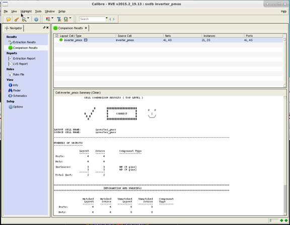
So now your layout is complete. Now we need to check it to make sure it is the same as the schematic that we did in the previous example. Select Calibre->Run LVS… The LVS window will pop up. Under Inputs, Netlist, check ‘Export from schematic viewer’. Run the LVS.
If your netlists match, your LVS screen will have a smiley face and will not have any error descriptions under Comparison Results.