EXAMPLE:
LAYOUT OF AN INVERTING AMPLIFIER
This example will help you to create a layout
for the inverter you designed in the first example. It will go over how to
create mosfets, resistors,
and capacitors in our process. There are many considerations to take into
account when deciding how to do a layout. This is NOT an example on layout
techniques, but more of a generalized example to help get you farmiliar with Virtuoso and
laying-out some basic components.
The following picture shows a layout for the inverting amplifier, ready for
extracting. The next section explains how to make each of the seperate components in Virtuoso.
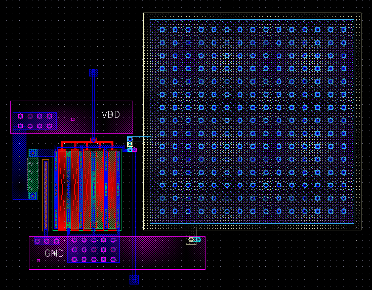
Figure 1: Layout example.
1. Create a new cell, where you will layout the inverter:
In Library Manager:
Highlight your inverter schematic library (TEST if
that is what you chose).
File->New->Cellview
Choose library TEST, cell name "inverter", view name
"layout", and Type: Layout and Application open with " Layout L". Click
OK.
2. Laying-out the components for your circuit:
For this inverter we will need to layout an nmos transistor, a resistor, and a capacitor. The following sections will describe how to make these components.
2.1 Layout of MOSFETs:
When
laying-out MOSFETs, we
actually have preset cells which we can draw from.
From the Layout window:
Create->Instance
Browse the library name, choose your library name (TEST for example), choose nmos from the Cell, and layout
from the View.
Click back on the Create Instance window to setup some parameters.
When making MOSFETs you can create a single transistor, or use fingering or multipliers to create multiple transistors at once. Fingering makes transistors which are connected in series, mulpliers create transistors which are connected in parallel. For our layout we will be using a multiplier to make multiple transistors which will be connected to be equivalent to one really wide transistor.
Change the Multiplier box to 5.
Change the Width box to 12.0u M.
Change the Length box to 1.2u M.
You can now place the nmos layout wherever you would like.
Clicking SHIFT-F will show all levels and allow you to see inside the cell you just placed (CNTRL-F will change back to just showing the top level).
Now we need to connect together the drains, gates, and sources and place some bulk connections.
In the LSW window change the current layer to poly
(dg).
Create->Path
Now draw a poly path connecting one gate to another accross the top of the transistor block. Make the
path extend up alittle ways
from the top of the transistor block before going over and down. Repeat this
until all gates are connected together.
Repeat this process to using metal1 to
connect every other drain/source connection together across the top.
Do the same thing for the opposite every other drain/source along the bottom.
Your finished transistor should look similar to the following:
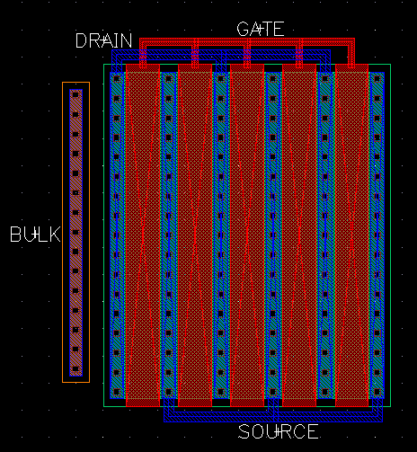
Figure 2: NMOS example.
Lastly we need to create some bulk connections. We will create these across the left side of the transistor block.
Create->Instance
Browse the library name, choose your library name (TEST for example), choose ptap from the Cell, and layout
from the View.
Click back over on the Create Instance window.
When placing instances you can place multiple instances in a matrix type formation by specifying the number of rows and columns to place. We will now use this to place a column of ptaps along the side of the transistor block.
In the Rows of contacts box put 15.
Place the block of ptaps
to the left of the transistor block.
We now have a transistor with single gate, drain, source, and bulk connections. Make sure to do DRC before continuing on to make sure everything was placed correctly.
2.2 Layout of Resistors:
There are several ways to make a resistor in layout. For a few reasons (issues with poly resistors using this design kit) we will make our resistors with nwell. Keep in mind that normally nwell resistors end up being nonlinear resistors, but for the purposes of this class (since we are simply doing LVS and extracting to Spetre) we will use them and consider them linear.
Create->Instance
Browse the library name, choose your library name (TEST for example), choose ntap from the Cell,
and layout from the View.
Place the cell on the layout.
An nwell transistor will extract at approximately 1.19k Ohms per square for our setup. The width of the nwell region is set by design rules to be atleast 1.44uM. This means to get the 4k resistor we want we will need a length of around 4.92uM. Also the nwell squares at each end of the resistor must be atleast 1.44uM squares, which means they also add 2.88uM to the length on the ends.
In the LSW window change the current layer to nwell (dg).
Window->Create
Ruler
Draw in a vertical ruler measuring 7.8uM. Draw
in a horizontal ruler off one of the corners measuring 1.44uM.
Create->Rectangle
Draw a rectangle of nwell
the size of the rules you just made.
Edit->Move
And move the ntap you made
previously to the centered end of one side of the rectangle.
Edit->Copy
And click on the ntap again to copy it and
move the copy down to the other side of the rectangle.
In the LSW window change the current layer to res_id(dg).
Now draw a rectangle of the res_id over the middle of the nwell. You will need to have it centered (0.24uM away from each NTAP edge) and the width of it atleast to the edges, if not overlapping them. Your finished product should look something like the following:
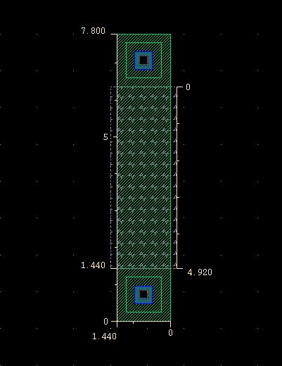
Figure 3: Resistor example.
We now have a resistor with metal1 connections on each side. Once again, make sure to do DRC before continuing on.
2.3 Layout of Capacitors:
The type of capacitor we will be making is called a mimcap. It is made up of two closely spaced layers of metal. For our setup the capacitor we will be making will have a capacitance of roughly 1fF per 1uM^2. For this reason most capacitors will be very large in comparison to some of your other components.
We need a 1pF load capacitor for our inverter. This works out to 1000uM^2. The square root of this sets each side to 31.6227uM if we decide on a square capacitor. Since our setup only goes in steps of .06uM, we will round down to 31.5uM.
Window->Create Ruler
Set a horizontal and vertical
ruler at 31.5uM each.
In the LSW window change the current layer to metalcap(dg).
Create->Rectangle
Draw a rectangle of metalcap
the size of the rules you just made.
Use the same steps to draw a rectangle of the layer metal5 directly ontop of the metalcap rectangle you just made.
Now we need to make a metal4 layer for the other side of the capacitor. This layer will need to be larger than the previous 2, by about 1uM on each edge.
Window->Create Ruler
Set a 1.02uM ruler (remember the .06uM steps) out from each edge of the
previous rectangles.
Now switch to the metal4 layer and draw a rectangle which is larger than the previous rectangles on all sides by 1.02uM.
We now need some contacts to connect the metalcap layer to the metal5 layer. This way we will have one connection of the capacitor from metal4 and one from metal5.
Create->Contact
Change Contact Type to M5_M4.
We will place multiple contacts to help fully connect the two layers.
Change the Rows box to 15.
Change the Columns box to 15.
Change the Delta X box to 2.02.
Change the Delta Y box to 2.02.
Now place the group of instances in the center of the metalcap/metal5 rectangle. If you dont get it like you want the first time, no worries, the whole group will move together when you adjust it's position later. Your finished capacitor should look something like this:
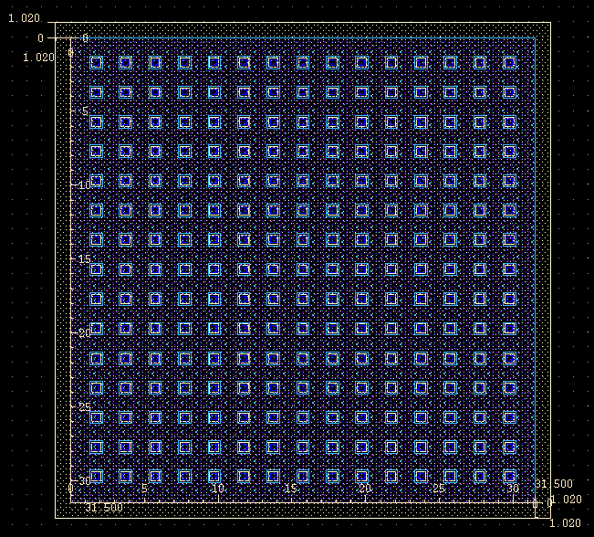
Figure 4: Capacitor example.
Now you have a capacitor with two terminals, the top at metal5 and the bottom at metal4. Remember, make sure to do DRC again to be sure you aren't violating any rules.
3. Routing and Adding Pins:
Now that we have all the components we need to make our inverter, we can simply move them around and route the correct connections. As mentioned earlier, this example is less focused on the techniques used for layout, and more on how to make some general components and get the reader familiar with using the tool. However, a couple quick pointers will be given here.
- When putting together your layout, place large metal rectangles (metal2 works well) along the top and botttom for your Vdd and Gnd rails. Try to place all of your layout within these rails. Also, when connecting to these (or any routing connection really) its always a good idea to put as many via connections as possible. You can use the same multiple contact placement as was used with the capacitor to make this fast and neat.
- Although it's not really obvious from this example, it is also good practice to try and make your layout as symetrical as possible.
- When routing large layouts it's a good idea to try and keep track of what you are routing with. Route with poly as little as possible since it's resistance is higher than metal. It also helps to set some general directions for different layers. For instance, for all horizontal traces use metal2, for all vertical traces use metal1. This will help keep your layout neat and organized.
After routing all your connections for the inverter (don't forget to DRC often), you simply need to add pins for vin, vout, vdd!, and gnd!.
Create->Pin
Type the Terminal Name, such as vin.
Select the I/O Type, such as "input" (although inputOutput is always a safe bet if unsure).
Check the Display Pin Name box.
Select the Pin Type based on what layer your connection is (Vdd and Gnd
should be metal2 if that is your rail's layer).
Simply place the pin and pin label where you want them.
After doing this for all the nodes your layout is complete!
4. Extraction and LVS:
So now your layout is complete. Now we need to check it to make sure it is the same as the schematic that we did in the previous example. First, extract the layout using the procedure described previously.
Now open the newly saved extracted view (placed in the same Cell as your layout), and go through the procedure for LVS described before. If all goes well your netlists will match!
5. Simulating the Layout:
We are almost done now, the only thing left is to simulate the extracted view of the inverter with the associated parasitics. This simulation will more accurately predict the behavior of the fabricated silicon. Since our cell layout is very small it is likely that the parasitics are so small that no significant simulation differences will be observed but in general the differences can be substantial for large complicated layouts.
First you need to create a symbol for your cell, in case you don't already have one, with Design -> Create Cellview -> From Cellview in the Composer window (from the original schematic) . Then create a new cell schematic that you can call "testbench" that contains only your cell (as a symbol) with input and output ports and supply symbols (vdd and gnd). To learn more about this, see the section about creating symbols.
Now let's start Analog Artist, in the newly created "testbench" cell window go to Tools -> Analog Environment, then in the Analog Environment window go to Setup -> Environment. The line that we need to change is called the Switch View List. This entry is an ordered list of cell views that contain information that can be simulated. The simulator (in fact the netlister) will search until it finds one of these cellviews. The default entry does not contain an extracted cellview. We need to add an entry for extracted cellview in front of the schematic cellview. As a result of this modification, the simulator will use the extracted cell view of the cell, if one is available. Click OK.
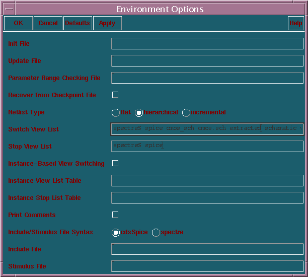
Now you can continue exactly as in the simulation tutorial and the only difference will be that you are simulating the extracted view (with the parasitics) and not the schematic view. Refer to the section about simulation.