cp /home/class/siva0024/NCSU-FreePDK45-1.2.tar .1.2 Extract the archive using the command
tar -xvf NCSU-FreePDK45-1.2.tar1.3 You should now be able to see a directory called FreePDK45 in your home directory. This directory contains an open-source, Open-Acess based PDK for the 45nm technology node and the predictive technology model which you will be using throughout this course.
cd ~/FreePDK45/ncsu_basekit/cdssetupHere, you will have to modify 2 files - cds.lib and setup.csh using vi, nano or any of your favorite editors as follows:
DEFINE freepdk_cells $PDK_DIR/osu_soc/lib/freepdk45_cells1.6 Modify setup.csh as follows:
1.6.1 Comment out the line which defines the environment variable PDK_DIR. Lines can be commented out by adding a # at the beginning.1.7 Create your temporary Cadence work directory
1.6.2 Set the PDK_DIR variable to the root directory of the FreePDK distribution
setenv PDK_DIR /home/class/use_your_username_here/FreePDK45
1.6.3 Comment out the line which defines the environment variable CDSHOME
1.6.4 Set the CDSHOME variable to the root directory the Cadence installation
setenv CDSHOME /home/vlsilab/cadence/ic611
1.6.5 Save and exit the file. Your process design kit is setup and ready to be used now.
mkdir cds_ncsu1.8 Copy setup.csh(the file you modified in step 1.6) into this directory
cd cds_ncsu
Always run Cadence from this directory to avoid cluttering up your workspace
cp ~/FreePDK45/ncsu_basekit/cdssetup/setup.csh .Source this script using the following command
source setup.csh1.8 Invoke Cadence by typing virtuoso &. This should bring up the command interface window and library manager. You are now ready to design circuits in Cadence.
This script copies the files needed by Cadence and initializes the environment.
q – Edit property of object
i – Create instance
w – Add wires
m – Move
c – Copy
s – Stretch
r – Rotate
z – Zoom in
Z – Zoom out
u – Undo
X – Descend edit
x – Descend read
b – Return
e – Display
From Virtuoso,
        File->New->Library
        Type a new name(I used "sample" and this is what I will refer to from here on).
        Select the "Attach to an existing technology library" option, click OK.
        Then in the popup window, select NCSU_TechLib_FreePDK45 and click OK
In Virtuoso command window, you will see the following messages (among other warnings) if everything is OK Created library "sample" as "/home/class/your_user_name/cds_freepdk/sample"
Design library 'sample' successfully attacjed to technology library 'NCSU_TechLib_FreePDK45'
        File->New->Cellview
        In the popup window, select "sample" (or the name of the library you created in step 1.1).
        Cell name "inverter". view name "schematic" and open with "Schematics L". Click Ok
        Click "Always" if "Upgrade License" warning message shows up. Virtuoso schematic editor opens up.
        Remember that anytime you get an Upgrade license warning, select the "Always/Yes" option everytime.
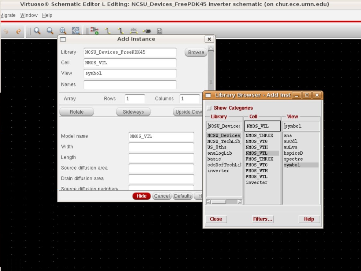
Make sure the Library in the library browser is set to NCSU_Devices_FreePDK45. Use the library browser window and click on NMOS_VTL, then select the symbol view.
You can now enter the width and length of the transistor in the Add Instance window. Use the same procedure for PMOS transistors. Also, from the library Basic, you can get the symbols for VDD and GND (they define the net names for the power and ground nodes)
If you make any mistake, you can always use
Edit->Delete or
Edit->Rotate or
Edit->Move or
Edit->Stretch
To change the properties of some of the components:
Edit->Properties->Objects
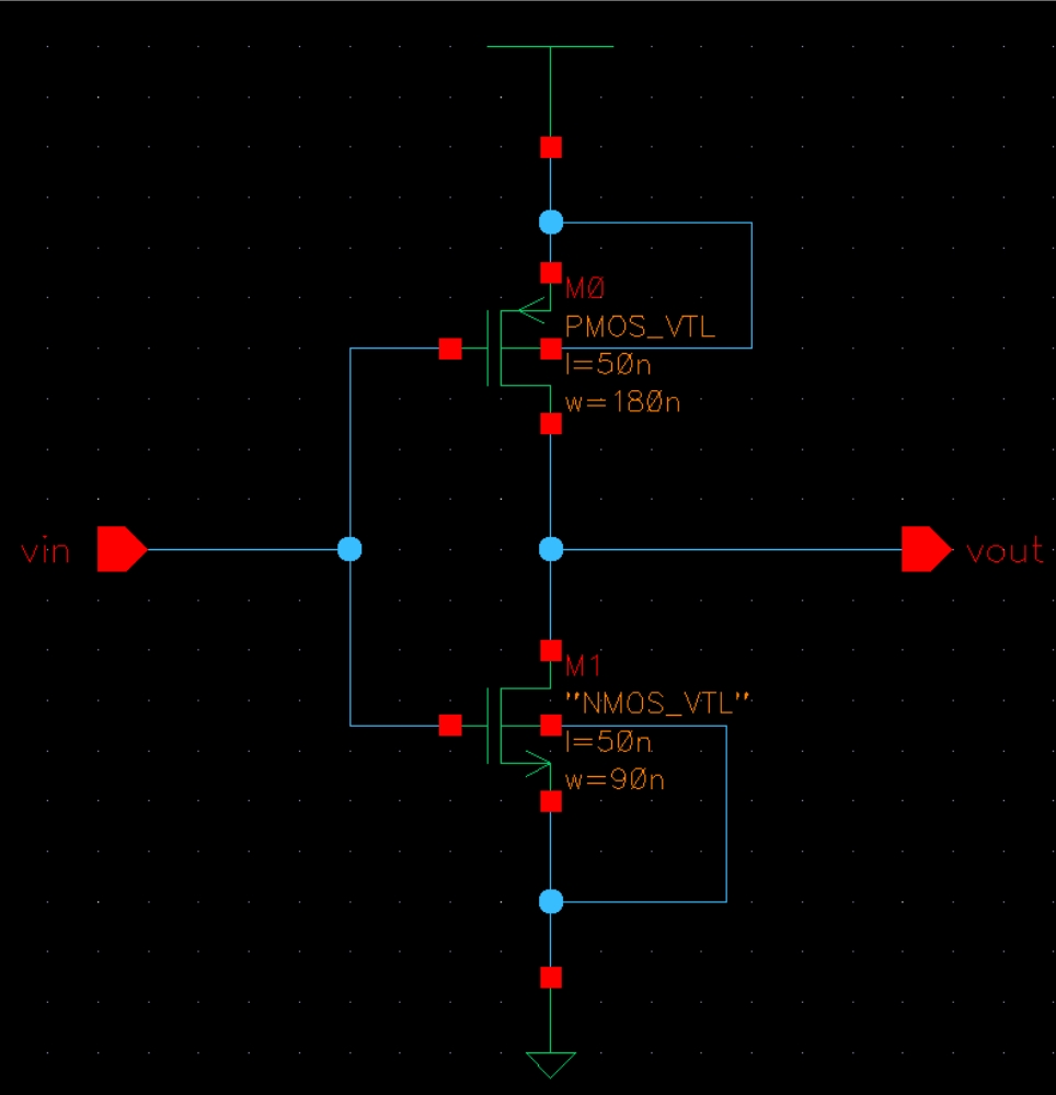
Select the NMOS_VTL transistor and make sure the width and length are
set to 90.0n M and 50.0n M respectively. If not, you can change the
properties of the transistor.
Similarly, set the width and length of the PMOS_VTL transistor to 180.0n M and 50.0n M.
        Design->Check and Save
        There should be no errors.
        Launch->ADE L
The window of Cadence Analog Design Environment will show up. Setup->Simulator/Directory Host
Set the simulator to hspiceD
Simulation->Netlist->Create
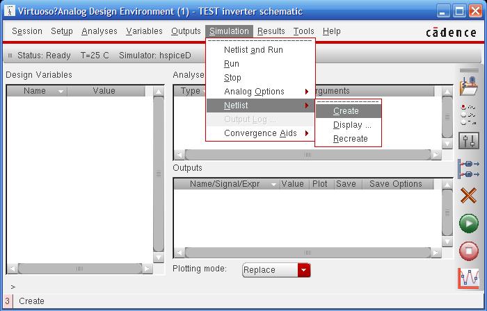
A new window will pop up showing the generated HSPICE netlist. You may save this file by clicking the menu bar:
File->Save As
Specify the full path name and file name in the Save As window.
For example, if we want save the file into a folder named "simulation"
under folder "~/cds_ncsu", we should type in
"~/cds_ncsu/simulation/inverter.sp". And the file name is "inverter.sp".
If you do not provide a path before file name, the file will be saved
under the folder where you start your Cadence.
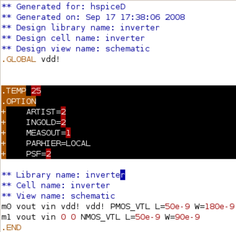
Now we have the netlist ready for editing and simulating. Open
the netlist in an editor and comment out the lines that are highlighted
in the above picture. You can comment lines in
a SPICE netlist by using *. Save the netlist and exit the editor.
Create another SPICE file named "runinv.sp" as below for simulation. It
should contain the part of the SPICE file inverter.sp that you commented
out in the previous step. You also need to include the models for the
transistors and the generated netlist file "inverter.sp".
. Finally you provide the values for the input and VDD.
**Test inverter
.TEMP 25
.OPTION
+            ARTIST=2
+            INGOLD=2
+            MEASOUT=1
+            PARHIER=LOCAL
+            PSF=2
+            POST
.inc '/home/class/your_user_name/FreePDK45/ncsu_basekit/models/hspice/tran_models/models_nom/NMOS_VTL.inc
.inc '/home/class/your_user_name/FreePDK45/ncsu_basekit/models/hspice/tran_models/models_nom/PMOS_VTL.inc
.include inverter.sp

v1 vdd! 0 1.1v
v2 vin 0 pwl 0ns 0 1ns 0 1.02ns 2.5 2ns 2.5 2.02ns 0 2.5ns 0
.op
.tran 0.01n 3ns
.end
Save the file “runinv.sp” and Exit the editor. The reason for using a separate file for simulation is because later on your circuit netlist may change, but the simulation file can be kept the same.
hspice runinv.spIf you have followed all the steps correctly, you will see the following message:
Using: /home/vlsilab/synopsys/hspice_2007.03-SP1/hspice/linux/hspice
 ****** HSPICE - Z-2007.03-SP1 32-BIT (May 25 2007) 18:56:14 09/03/2008 linux
  Copyright (C) 2007 Synopsys, Inc. All Rights Reserved.
  ...
  ...
  ...
  ***** job concluded
1 ****** HSPICE - Z-2007.03-SP1 32-BIT (May 25 2007) 18:56:14 09/03/2008 linux
 ******
 ** test inverter
 ...
 ...
 ...
 Init: hspice initialization file: /home/vlsilab/synopsys/hspice/hspice.ini
 lic: Release hspice token(s)
HSPICE job runinv.sp completed.
The important message is the “job concluded”. If the job is “aborted”, you will have to debug the errors in your netlist. For detailed HSPICE command and syntax, the readers are referred to the HSPICE manual on the class webpage.
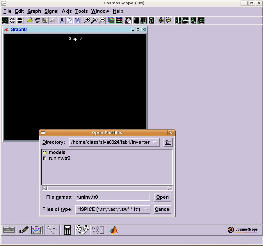
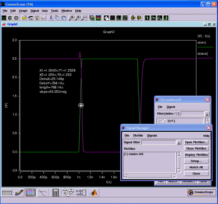
In the results browser window, double click "v(vin)" and "v(vout)" to plot the waveforms of the signals.
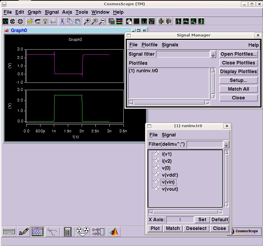
You can measure the propagation delay by
1) Drag the v(vout) signal into the same window as v(vin) signal;
2) Select both "vin" and "vout" signals using control key;
3) Click the second but last button on the tool bar;
4) Drag the start and end circles to the location you want to measure;
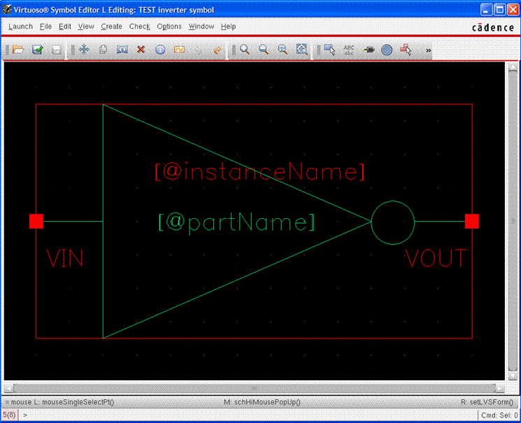
A new window will open with the symbol view. By default, the symbol shape is a rectangle, but you can change it. Since this design is an inverter, we will draw a triangle and put a small circle at the output. To do this, you will want to delete the green rectangle, draw the new shape, and move the terminals to new positions. Use Create->Shape to draw a triangle and place a circle. There are several shapes available: line, rectangle, circle, etc. You will also need to change the Selection box (the red rectangle), which defines the limits of the symbol. This can be done by stretching the Selection box. Figure below shows an example of the inverter symbol:
Don't forget to check and save.
To move in the hierarchy, select the inverter, and then:
Edit->Hierarchy->Descend Edit
You can choose the schematic or the symbol for editing.
To return to the previous schematic, use:
Edit->Hierarchy->Return
The following picture shows the layout of the inverter. The rest of the section explains how to make each of the separate components in Virtuoso.
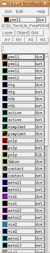
You can draw a shape by first selecting the layer from the LSW, then Create->shape->.... You will be drawing rectangles for the most part. Note that this is similar to how you created symbols in Section 1.8.
An NMOS transistor uses the following layers: pwell, active, nimplant, poly, metal1 & contact..
You can start designing the transistor by selecting "active" on the LSW
and drawing a rectangle on the layout editor. Note also the letters
"drw", "net", and "pin" next to each entry in the LSW. These are the
purposes of a shape. The purpose is used to indicate special
functionality of a shape. We will be using "drw" for now.
At this point, do not worry about drawing the rectangle to exact
dimensions and just draw a rectangle of any arbitrary dimension. You can
zoom in and out of the editor by using the zoom buttons located on the
top menubar of the editor. You can also draw a box around the area you
want to zoom in by holding on to your right mouse click button. When you
release the button, the area you selected will be zoomed in.
Once you draw the rectangle, you can select it and press "q" or Edit->Basic->Properties to change the dimensions of the rectangle.
. You can move objects around by pressing "m" or Edit->move. Readers are strongly encouraged to get familiar with other keyboard shortcuts as this will reduce design time later on.
The default units are "user units" and are in microns. For our inverter,
the NMOS transistor has a width of 90n M. So, make sure that the active
layer that you have just now drawn is also 90n M in width. Then you
repeat the same process but by selecting the "nimplant" layer from the
LSW. The active and nimplant layers must overlap and these form the
Source and Drain diffusion regions of the NMOS transistor you are trying
to create. The following pictures illustrate these two steps.
The next step is to draw the gate of the transistor. This is
done by selecting "poly" in the LSW and drawing another rectangle to
form the gate. Make sure that the length of the gate is set to 50n M to
create the transistor that we used for the schematic. Now, we have
formed the channel and the source and drain diffusion regions. The next
step is to draw a pwell outside the NMOS transistor. Use the same
procedure as described earlier to draw the pwell. The resulting
transistor is shown in in the following picture
.
We still have to create contacts for the source, drain and the
body terminals of the transistor. You can create contacts to the active
layer by selecting "contact" from the LSW and painting a rectange on the
Active layer. Paint two contacts for the Source and Drain regions of
the transistor. Now you need to create a body terminal. To do this,
click on Create->via or press "o". In the window that opens up, make sure that the Technology Library is set to NCSU_TechLib_FreePDK45 and select "PTAP" in the Via Definition field. Place the PTAP connection in contact with the pwell you have drawn. You can press Shift+F to reveal the details inside the PTAP connection.
Draw metal1 rectangles over the contacts so that you can connect the
terminals to other signals in your circuit. Your NMOS transistor is now
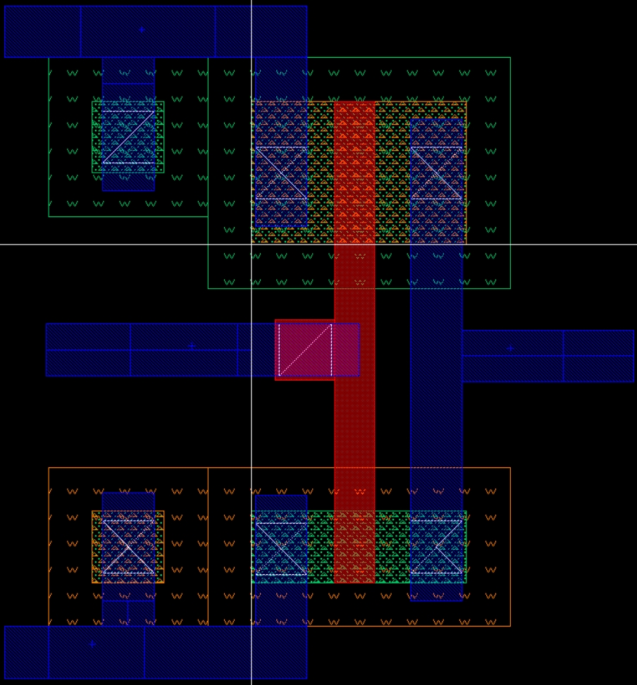
ready. The final transistor should look like the following picture.
![]()
You can create the PMOS transistor similarly. It uses the following layers:nwell, active, pimplant, poly, metal1 & contact. Make sure the dimensions of the PMOS transistor match that used in the schematic.
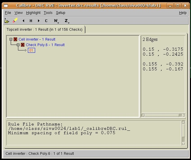
The presence of a red check mark in the DRC results window
indicates that the layout failed the DRC check. The results window give
information on what design rule was violated, where it was violated and
how many instances have violated the rule.
In the topmost level in the results window, it says "Cell Inverter - 1
Result". This means that there is one instance of a design rule being
violated somewhere in the layout. Underneath that, it says "check
Poly.6" 1 Result. This is the design rule being violated.
In the message window below, it says that " Minimum spacing of field
poly = 0.075". This means that somewhere in the design, we have 2 pieces
of poly that are closer than 0.075 microns and this violates the design
rule of the process.
The following picture shows a zoomed in version of our poly connections.
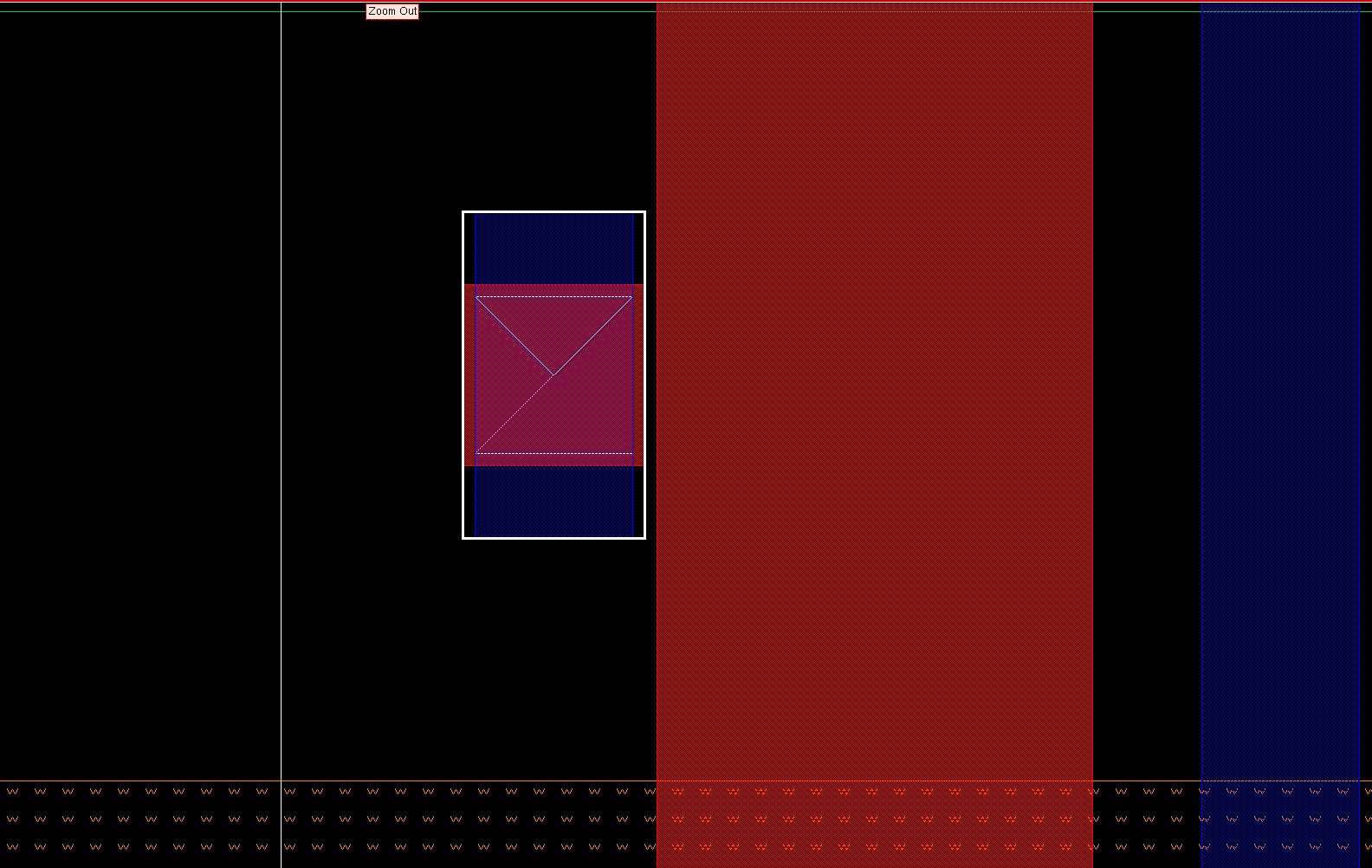
You can observe that there is a small gap between the poly
connecting the gates of the two transistors and the M1_Poly contact.
This resulted in the layout failing the DRC check. You can fix this
error by moving the M1_Poly to the right so that gets in contact with
the poly connecting the gates.
The following picture shows the results of the DRC when you fix this problem and re-run DRC.
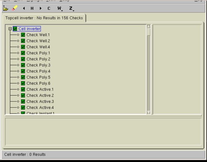
Note that when you are working through this tutorial you may get other errors from DRC. You can get more information about design rules from the link posted earlier in this section or from the NCSU wiki page linked at the bottom of this page. The DRC results window will let you know what rules you have violated. So, in conjunction with the set of design rules in the wiki you can fix those errors.
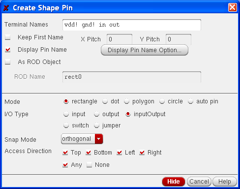
Next, click the "Display Pin Name Option..." button. You will see another dialog box appear.
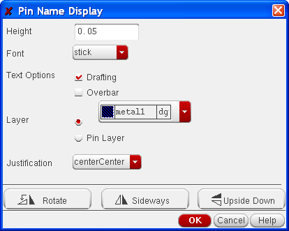
Set the height to 0.05 um and the layer to metal-1 dg. Click OK.
Next, click on layout where you want each pin to be placed. You will
need to click three times: twice to create a rectangle for the pin and a
third time to place the label. The shape of your rectange does not
matter as long as it only covers area that is already covered by
metal1-dg. Re-run DRC to make sure the layout passes all design rules.
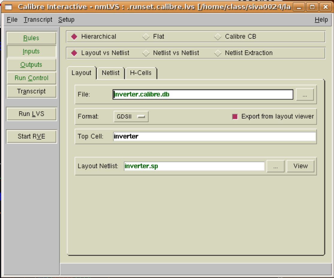
Make sure you select the "Export from layout viewer" option under the Layout tab and "Export from schematic viewer" under the Netlist tab. Under the Outputs
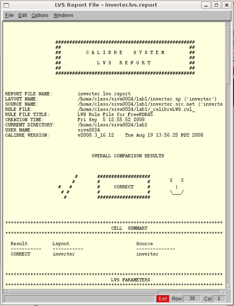
tab, set the svdb directory to svdb_inverter. Then click on "Run LVS"
button. If LVS runs sucessfully, then you will see the following window
with a smilie.
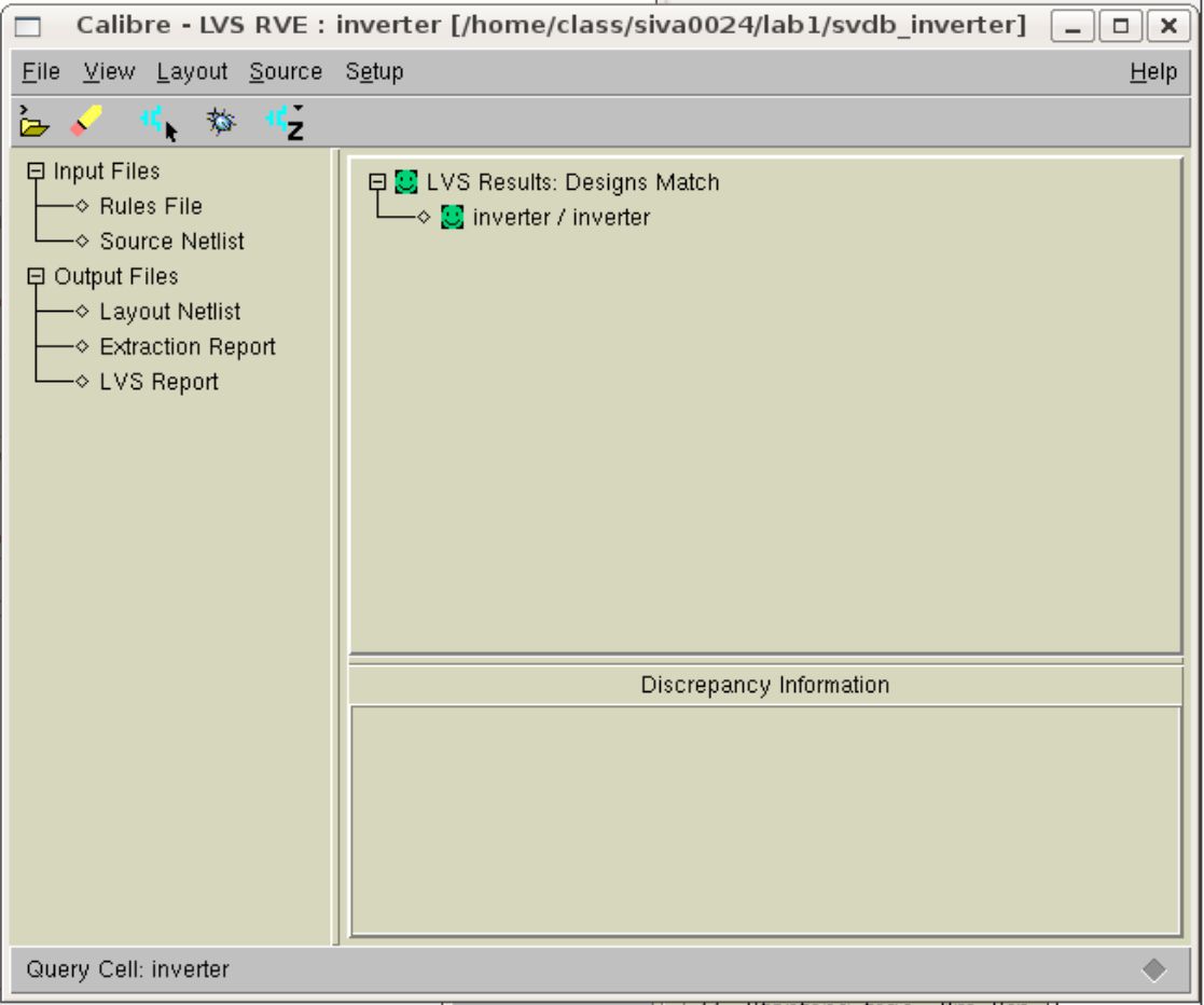
Click on "Transcript" tab in Calibre Interactive - LVS to see the log file. The LVS report is also opened and is shown below.