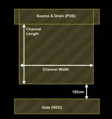
Note: The capacitor supported in this design kit is formed in the way of a PTFT with P3HT-channel. Therefore, it has positive (drain and source) and negative (gate) ends.
A. METAL1
In the LSW window, choose METAL1 (drw). From the Layout window, choose
Create->Shape->Rectangle
1. Draw the positive end. Assume we are going to draw a TFTCAP of 2uF. Since the unit capacitance is 10pF/(sq um), we can use W/L = 500um/400um. Draw a rectangle of 500um x 500um, and draw another of 550um x 100um, placed on top of the first one, overlapping 100um in Y direction. Thus only 500um x 400um is going to be used as the capacitor plate.
2. Draw the negative end. Draw a rectangle of 550um x 100um, placed under the 500um x 500um one, with 100um distance away in Y direction.
The final pattern should look like this:

B. P3HT Channel
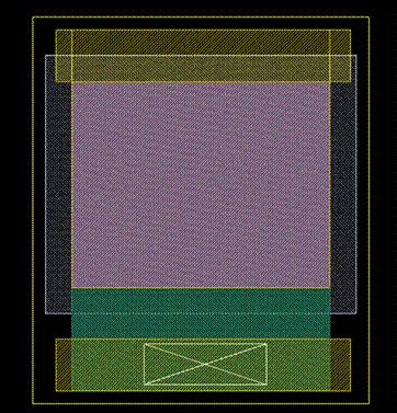
Select P3HT_CAP (drw) from LSW window, and draw a rectangle of 500um x 400um, covering the entire 500um x 400um METAL1 plate. This is the dielectric layer of the TFTCAP.
C. Ion-Gel Dielectric
Select IONGEL_CAP (drw) from LSW window, and draw a rectangle of 600um x 500um, completely enclosing the P3HT plate, with 50um extension on four edges.
D. PEDOT Conductive Layer
Select PEDOT_CAP (drw) from LSW window, and draw a rectangle of 500um x 600um, completely enclosing the P3HT plate, and overlapping with the negative end with 100um.
E. Contact
For LVS purpose, dummy contacts are required in layout. Select CONTACT (drw) from LSW window and draw a rectangle at negative end (PEDOT overlapping METAL1).
F. Substrate
For LVS purpose, substrate layer is required in layout. Select SUB (drw) from LSW window and draw a rectangle to enclose everything.
The final layout should be like this:
