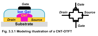
Note: CNT TFTs are neither P-type nor N-type. The corresponding device is modeled as a PTFT_CNT_TG and a NTFT_CNT_TG connected in parallel.

A. METAL1
In the LSW window, choose METAL1 (drw). From the Layout window, choose
Create->Shape->Rectangle
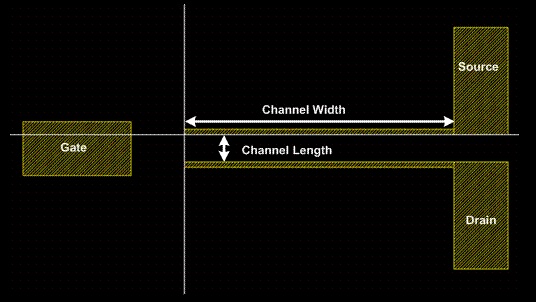
1. Draw the source/drain electrodes. Assume we are going to draw a TFT with W/L = 500um/50um, with a source/drain electrode width of 10um. Draw a rectangle of 500um x 10um, and draw another under the first rectangle, with 50um distance in between.
2. Draw the source/drain connections to other nets. On the right side of the drawn electrodes, draw two rectangles in METAL1, each being 100um x 200um.
3. Draw the gate electrode. On the left side of the drawn electrodes, draw a rectangle of 200um x 100um in METAL1, with 100um distance away from the source/drain electrodes.
The final pattern should look like this:

B. CNT Channel
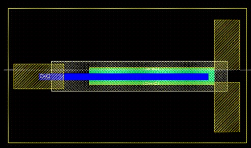
Select CNT_TFT (drw) from LSW window, and draw a rectangle of 500um x 120um, covering the entire two source/drain electrodes and filling the entire 50um gap to form a channel.
C. CNT Dummy Channel Layer
Since CNT TFTs are modeled as a P-type and a N-type TFT connected in parallel, a dummy channel layer is required to represent the N-type device model (the CNT channel layer in Step B represents the P-type device). Select CNT_TFT_DUM (drw) from LSW window, and draw a rectangle of 500um x 120um, exactly overlapping with the CNT_TFT layer in Step B.
D. Ion-Gel Dielectric
Select IONGEL_TFT (drw) from LSW window, and draw a rectangle of 700um x 120um, completely enclosing the CNT channel, with 25um extension on the length direction and 50um extension on the width side onto METAL1.
E. PEDOT Conductive Layer
Select PEDOT_TFT (drw) from LSW window, and draw a rectangle of 675um x 25um, placed roughly in the middle of the channel. Locate the rectangle so that it extends onto METAL1 over Iongel layer on the gate side by 50um. Iongel layer should also enclose this PEDOT layer by 25um on the right side.
F. Contact
For LVS purpose, dummy contacts are required in layout. Select COTFT (drw) from LSW window and draw rectangles at source (CNT overlapping METAL1), drain (CNT overlapping METAL1). Select CONTACT (drw) from LSW window for rectangles at gate (PEDOT overlapping METAL1 but not interacting with IONGEL).
G. Substrate
For LVS purpose, substrate layer is required in layout. Select SUB (drw) from LSW window and draw a rectangle to enclose everything.
The final layout should be like this:
